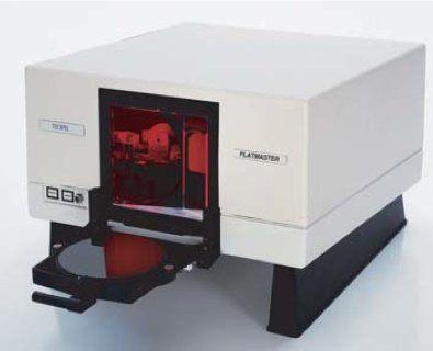
Tropel FlatMaster Wafer Form Analysis System
Fast and precise wafer flatness measurements.

Tropel FlatMaster® Wafer systems use a wide range of easy-to-load wafer chucks to allow clamped or free-state measurements. Windows®-based software simultaneously tests wafers to multiple user-definable global and local site flatness parameters. The continued demand for higher-density chips with smaller critical dimensions leads to tighter substrate form tolerances both on the global and the individual die-site scale.
The patented grazing-incidence interferometry technology optimized for the highest precision flatness measurements makes this the ideal system for processes development, particularly for new, non-silicon materials. From wire saw to finished wafer, you can quickly and accurately measure flatness to verify that you have the ability to achieve the required device yields.
The surface metrology machine measures flatness, taper, thickness variation, thickness, stress, bow, warp, SORI, and many other parameters including stepper simulation of any surface. Combined with state of the art optical fabrication techniques and Tropel's renowned phase-shifting analysis software, the FlatMaster Wafer offers full-form surface information with 50-nanometer accuracy in seconds.
Browse our Catalog to learn more about the Tropel FlatMaster Wafer Form Analysis System and other metrology instruments.