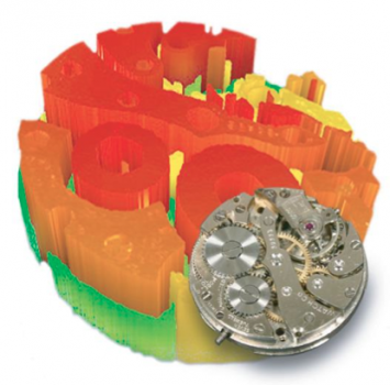
Industrial Manufacturing
FlatMaster MSP
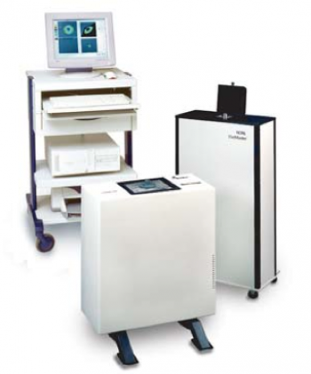
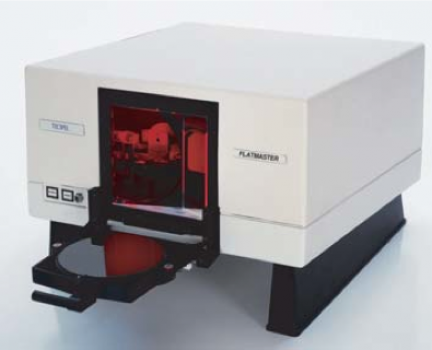
FlatMaster MSP 150
The Tropel® FlatMaster® MSP (Multi Surface Profile) Optical Metrology System is a non-contact, frequency scanning interferometer, capable of measuring precision parts with multiple surfaces. It allows you to measure flatness, parallelism and height/depth on a variety of materials and surface finishes in just seconds, with sub-micron accuracy, providing considerable value to your production needs.
Learn more about the Tropel FlatMaster MSP Optical Metrology System.
FlatMaster MSP 40
The Tropel® FlatMaster® MSP (Multi Surface Profile) Optical Metrology System is a non-contact, frequency scanning interferometer, capable of measuring precision parts with multiple surfaces. It allows you to measure flatness, parallelism and height/depth on a variety of materials and surface finishes in just seconds, with sub-micron accuracy, providing considerable value to your production needs.
Learn more about the Tropel FlatMaster MSP Optical Metrology System.
FlatMaster Roughness
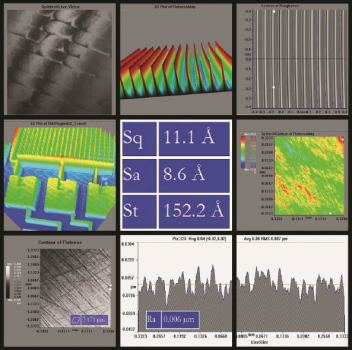
FlatMaster System with Surface Roughness Measurement
The Tropel FlatMaster System with Surface Roughness Measurement measures a broad variety of materials and surface finishes for a characteristics such as lay, roughness, and all standard profile parameters for 2D and 3D standards. By simply placing the part on the system, you will have a full profile analysis in seconds, allowing you to ensure product quality while minimizing risks and lowering manufacturing costs.
Learn more about the Tropel FlatMaster System with Surface Roughness Measurement.
FlatMaster Surface
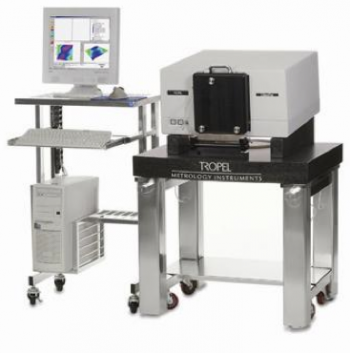
FlatMaster Surface 100
The Tropel® FlatMaster® provides industry-leading performance of surface form measurements for precision component manufacturers. The non-contact optical technique records the entire surface in seconds. It offers five nanometer resolution and a standard accuracy of 50 nanometers. It rapidly and accurately measures flatness, line profile, radius and other surface parameters from a variety of surfaces.
Learn more about the Tropel FlatMaster Surface Form Analysis Systems.
FlatMaster Surface 200
The Tropel® FlatMaster® provides industry-leading performance of surface form measurements for precision component manufacturers. The non-contact optical technique records the entire surface in seconds. It offers five nanometer resolution and a standard accuracy of 50 nanometers. It rapidly and accurately measures flatness, line profile, radius and other surface parameters from a variety of surfaces.
Learn more about the Tropel FlatMaster Surface Form Analysis Systems.
FlatMaster Surface 40
The Tropel® FlatMaster® provides industry-leading performance of surface form measurements for precision component manufacturers. The non-contact optical technique records the entire surface in seconds. It offers five nanometer resolution and a standard accuracy of 50 nanometers. It rapidly and accurately measures flatness, line profile, radius and other surface parameters from a variety of surfaces.
Learn more about the Tropel FlatMaster Surface Form Analysis Systems.
UltraFlat
UltraFlat 200
The Corning Tropel Corporation designed the Tropel® UltraFlat 200 Mask System specifically for the photomask industry. It delivers the lowest measurement uncertainty for ever-tightening mask flatness specifications. Shrinking device features require not only flatter wafers, but flatter masks, as small devices require flatness. The UltraFlat system is used to measure flatness of photoblanks and photomasks throughout every stage of manufacturing and use.
Learn more about the Tropel UltraFlat 200 Mask System.
Semiconductors
FlatMaster Wafer
FlatMaster Wafer 100
The Tropel FlatMaster® Wafer systems use a wide range of easy-to-load wafer chucks to allow clamped or free- state measurements. Windows®-based software simultaneously tests wafers to multiple user-definable global and local site flatness parameters. The continued demand for higher density chips with smaller critical dimensions leads to tighter substrate form tolerances both on the global and the individual die-site scale.
Learn more about the Tropel FlatMaster Wafer Form Analysis System.
FlatMaster Wafer 200
FlatMaster® Wafer systems use a wide range of easy-to-load wafer chucks to allow clamped or free- state measurements. Windows®-based software simultaneously tests wafers to multiple user-definable global and local site flatness parameters. The continued demand for higher density chips with smaller critical dimensions leads to tighter substrate form tolerances both on the global and the individual die-site scale.
Learn more about the Tropel FlatMaster Wafer Form Analysis System.
UltraSort
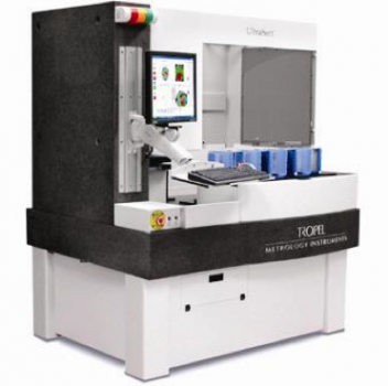
UltraSort
The Corning Tropel UltraSort represents the State Of The Art in automated semiconductor wafer measurement, and continues a 25 year tradition of providing metrology solutions to semiconductor manufacturers. Designed specifically for high volume wafer manufacturing, this automated system offers the utmost in rapid, repeatable, accurate non-contact verification of many substrate materials in the field.
Learn more about the Tropel UltraSort.